Explore our custom OEM transient suppression solutions, high-power SCRs, fast recovery rectifiers, and high-voltage silicon stacks engineered for extreme electrical environments.
In modern industrial electrification, power conversion, and military electronics, transient voltage events pose catastrophic risks to sensitive semiconductors. Transient Voltage Suppressors (TVS) act as clamping devices that absorb destructive electrical overstress (EOS) caused by lightning strikes, inductive load switching (such as motor relay disconnections), electrostatic discharge (ESD), and electromagnetic pulses (EMP). As a premier custom OEM transient suppressor manufacturer and supplier, our engineering philosophy focuses on sub-nanosecond response times, precise clamping voltage ratios ($V_C / V_{BR}$), and zero-degradation avalanche junction mechanisms.
Silicon TVS devices operate on the principle of p-n junction avalanche breakdown. Under nominal operating conditions, the TVS presents a high impedance to the circuit, drawing minimal reverse leakage current ($I_R$). When a transient voltage spike exceeds the reverse breakdown threshold ($V_{BR}$), the semiconductor junction transitions into a low-impedance avalanche state, shunting the surge current ($I_{PP}$) safely to ground while clamping the output voltage to a safe level ($V_C$). This protective action prevents the breakdown of downstream integrated circuits, power MOSFETs, and IGBT gates.
Unlike MOV or GDT devices, solid-state silicon TVS junctions respond virtually instantly (<1 picosecond), clamping ESD and fast transients (EFT) before voltage overshoot harms sensitive logic.
Our proprietary silicon die doping profiles minimize dynamic resistance ($R_{DYN}$), ensuring the ratio of maximum clamping voltage ($V_C$) to breakdown voltage ($V_{BR}$) stays ultra-tight under peak surge conditions.
Designed for lifetime continuous protection, our avalanche TVS diodes do not wear out or experience structural aging over millions of transient discharge cycles when operated within specification.
Comparing different transient suppression technologies reveals why custom silicon TVS and hybrid active thyristor/rectifier protection networks remain the gold standard for high-reliability industrial and defense programs:
| Suppression Technology | Response Time | Clamping Performance | Degradation Over Time | Capacitance Range | Ideal Application Sector |
|---|---|---|---|---|---|
| Silicon TVS Diode Stacks | < 1 picosecond | Excellent (Tightly Clamped) | None (Solid State Avalanche) | Low to Medium (Customizable) | High-Rel Aerospace, Defense, Telecom, Process Controls |
| Silicon Controlled Rectifiers (SCR) | 10 - 100 nanoseconds | Crowbar (Diverts Voltage to Zero) | None (High Energy Capacity) | Medium | Industrial Motor Drives, HV Braking, Power Conversion |
| Metal Oxide Varistor (MOV) | 1 - 25 nanoseconds | Moderate (High $V_C / V_{BR}$ ratio) | High (Degrades with each surge) | High (> 1000 pF) | AC Mains Secondary Surge Protection |
| Gas Discharge Tube (GDT) | 100 - 500 nanoseconds | Crowbar (Slow Turn-on) | Moderate (Electrode Erosion) | Very Low (< 1 pF) | RF Lines, Lightning Primary Protection |
Standard off-the-shelf transient suppressors frequently fail to meet specialized electrical, thermal, or physical spatial constraints in demanding application environments. As a full-service custom OEM manufacturer, our engineering team works directly with tier-1 systems integrators to co-design custom transient suppressors, high-voltage rectifier blocks, and thyristor assemblies from the wafer-level silicon die up to the final potted module assembly.
Our OEM engineering lifecycle includes extensive thermal modelling, finite element analysis (FEA) of junction temperatures during peak surge discharge, and full compliance pre-testing against global surge immunity standards (IEC 61000-4-5, MIL-STD-704F, MIL-STD-1275E, DO-160G, AEC-Q101).
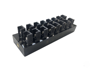
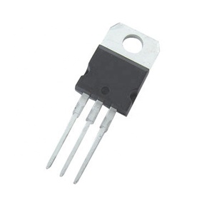
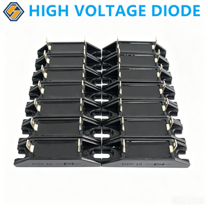
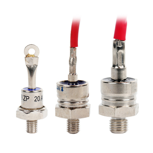
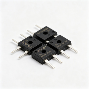
To assist power design engineers and procurement directors in choosing optimal components for their surge isolation and power conversion schematics, we present a granular technical breakdown of our core product architectures shown in our product showcase catalog above:
High voltage rectifier diode blocks are modular, multi-junction silicon assemblies designed for high voltage industrial equipment. Utilizing glass-passivated avalanche chip matrices, the 2CLG20KV/50A-WT series provides exceptional reverse voltage withstand strength up to 20kV with continuous forward current handling of 50A. Integrated transient suppression capability allows these diodes to withstand repetitive peak reverse surges without avalanche puncture, making them mandatory for high-voltage DC power supplies, X-ray generators, and industrial microwave plasma equipment.
Silicon Controlled Rectifiers (Thyristors) function as high-speed controllable electronic switches. In protection circuits, SCRs serve in "crowbar" surge protection roles. Upon detecting an overvoltage event on an industrial bus (such as 400VAC brake inputs), the SCR gate is triggered within nanoseconds, short-circuiting the power line and blowing a fast-acting fuse or shunting heavy current away from sensitive power converters. The M400 MGM OEM Brake SCR Module is specifically engineered for motor braking networks where inductive energy kickback from large electromagnetic coils must be dumped rapidly without damaging the main inverter bridge.
In high-frequency induction heating, radio frequency (RF) transmitters, and ozone generators, stray capacitive and inductive spikes frequently exceed tens of kilovolts. The HVP-16 17.5KV Silicon Stack integrates multiple series-connected avalanche-passivated diode chips encased in high-dielectric epoxy resin. Featuring ultra-fast reverse recovery times ($t_{rr}$), these stacks mitigate transient ringing and high-voltage ringing transients that destroy conventional power supply transformers.
High power rectification in heavy industrial electrochemical processes—such as chrome plating lines, copper electrowinning, and hydrogen electrolysis—demands extreme continuous current capabilities and rugged physical construction. The ZP100A 1600V Spiral Stud Diode utilizes a heavy-gauge copper stud with a spiral thread for ultra-low thermal resistance ($R_{\theta JC}$) when mounted directly to liquid-cooled or forced-air heatsinks. Its robust silicon structure tolerates high surge currents ($I_{FSM}$) up to several kiloamperes during AC line transient faults.
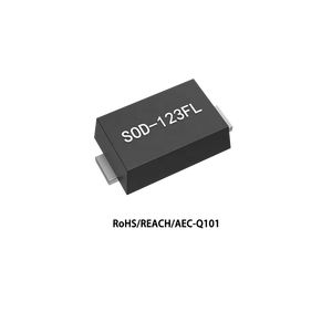
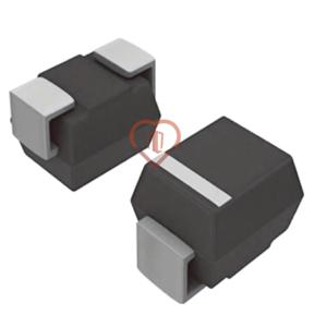
For modern surface-mount printed circuit board (PCB) layouts, miniaturization must not compromise transient withstand capability. The P0080TA-MC SMA series provides precise silicon zener/thyristor-based voltage clamping for telecom and consumer electronics protection, while the 1N4006W SOD-123FL series delivers compact general-purpose rectification with 100% original traceable lot coding, ensuring zero counterfeit component risk for military and medical OEM builds.
As industrial automation, renewable energy infrastructure, electric vehicle (EV) charging networks, and aerospace systems transition to higher operating voltages and wide-bandgap (SiC/GaN) semiconductors, transient voltage suppression requirements are undergoing a fundamental evolution. OEM buyers and system architects must align their supply chain and design choices with key macro trends:
Megawatt-scale green hydrogen electrolysers, solar PV farms, and EV ultra-fast charging hubs are migrating from traditional 400V/600V DC buses to 1000V–1500V DC lines. This shift requires high-voltage custom TVS stacks capable of handling immense energy discharges without excessive clamping overshoot.
Silicon Carbide MOSFETs switch exceptionally fast ($dv/dt > 50\,\text{V/ns}$), creating severe parasitic inductive voltage spikes across gate drives and power loops. Custom ultra-low inductance ($L_{PAR}$) TVS diodes are increasingly specified directly onto power module substrates to protect fragile SiC gate oxides.
With global supply chain vulnerabilities, aerospace, medical, and defense OEMs mandate 100% full wafer-to-packaged device traceability. Factory-direct lot coding, certified Certificate of Conformance (CoC), and wafer-level test reporting are becoming mandatory procurement prerequisites.
Adoption of severe surge immunity specifications—such as MIL-STD-1275E (28V DC input load dump surges up to 100V for 50ms) and ISO 7637-2 pulse waveforms—drives demand for custom high-energy TVS arrays replacing legacy active disconnect switches.
Building high-reliability transient suppression systems requires absolute manufacturing precision, rigorous material science controls, and continuous quality verification. We combine decades of semiconductor fabrication expertise with flexible OEM engineering service:
Every production run undergoes strict statistical process control (SPC), 100% parameter screening ($V_{BR}, I_R, V_C$), and thermal shock testing.
Laser-etched lot codes match raw silicon ingot certificates, guaranteeing genuine materials and anti-counterfeit assurance.
Accelerated custom sample manufacturing turns clean-sheet OEM requirements into fully qualified prototypes in as little as 3 to 4 weeks.
Comprehensive technical answers regarding custom TVS specifications, selection criteria, lead times, and qualification standards.
The required Peak Pulse Power ($P_{PP}$) is calculated by multiplying the maximum expected peak clamping voltage ($V_C$) by the peak pulse surge current ($I_{PP}$) under your target waveform standards—typically the standard $10/1000\,\mu\text{s}$ exponential impulse or the $8/20\,\mu\text{s}$ high-current lightning waveform (IEC 61000-4-5):
$$P_{PP} = V_C \times I_{PP}$$
For example, if your circuit must withstand a 100A surge under an $8/20\,\mu\text{s}$ pulse and the clamped voltage must not exceed 45V, the TVS junction must be engineered to handle a minimum peak power of $45\text{V} \times 100\text{A} = 4500\text{W} = 4.5\text{kW}$. Our custom silicon team optimizes die surface area to safely dissipate these energies without thermal runaway.
Reverse Standoff Voltage ($V_{RWM}$): The maximum continuous DC or peak AC operating voltage at which the transient suppressor remains in its non-conducting, high-impedance state. At $V_{RWM}$, the device draws only a small specified standby leakage current ($I_R$). Always select $V_{RWM}$ to be equal to or slightly greater than the maximum nominal supply voltage of your system rail.
Breakdown Voltage ($V_{BR}$): The voltage point at which the TVS diode junction begins conducting current and enters reverse avalanche breakdown, measured at a standardized test current ($I_T$, typically 1mA or 10mA). $V_{BR}$ is normally 10% to 15% higher than $V_{RWM}$.
Yes. We specialize in custom military COTS (MIL-COTS) and full MIL-SPEC transient protection assemblies designed to meet rigorous standards such as MIL-STD-704F (Aircraft Electric Power Characteristics), MIL-STD-1275E (Characteristics of 28V DC Electrical Systems in Military Vehicles), and MIL-STD-461 (EMC Controls). We offer specialized high-energy surge testing, burn-in screening, hermetic packaging, and full environmental qualification (MIL-STD-883).
Standard high-power TVS diodes feature relatively high internal p-n junction capacitance ($C_j > 500\text{ pF}$), which can severely distort high-frequency digital signals on data lines such as Industrial Ethernet, CAN Bus, RS-485, or USB 3.0. For signal line protection, our OEM plant fabricates low-capacitance TVS topologies by integrating steering diode bridges in series with the TVS avalanche element, dropping overall line-to-ground capacitance to less than $1\text{ pF}$ to $5\text{ pF}$ without sacrificing ESD/surge protection capability.
For custom variations based on existing semiconductor package footprints (such as custom $V_{BR}$ binning or customized lead form geometries), engineering prototype samples are typically delivered in 2 to 4 weeks. Completely clean-sheet custom die layouts, high-voltage multi-chip epoxy stacks, or custom mechanical housing fabrications generally require 6 to 8 weeks for qualified first-article samples. Volume production is supported with flexible buffer stocking programs, Kanban arrangements, and JIT delivery schedules.
Silicon TVS diodes exhibit a safe "fail-short" mode when subjected to excessive surge current or pulse duration exceeding their peak pulse power ratings. The silicon junction melts and forms a permanent conductive metal bridge, resulting in a low-resistance short circuit. This failsafe characteristic causes upstream fuses or circuit breakers to trip immediately, ensuring downstream sensitive microelectronics are completely isolated from un-clamped line voltages.
Connect directly with our senior power semiconductor application engineers. Share your voltage requirements, surge standards, packaging constraints, or target delivery dates for an immediate technical route evaluation and commercial proposal.