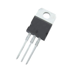
Explore our field-proven power semiconductor components engineered for high-frequency inversion, extreme dv/dt immunity, and demanding thermal industrial duty cycles.
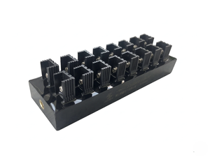
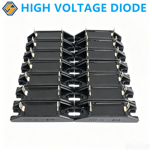
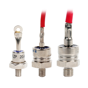
In modern high-frequency power electronics—ranging from megawatt-scale green hydrogen electrolyser power supplies and active front-end (AFE) motor drives to industrial induction heating and MIL-COTS energy systems—the power MOSFET (Metal-Oxide-Semiconductor Field-Effect Transistor) module serves as the critical switching backbone. Selecting a reliable MOSFET module manufacturer and exporter requires looking beyond standard parametric tables to evaluate die-level topology, substrate thermal management, parasitics, dynamic gate charge behavior, and long-term reliability under cyclic electro-thermal stress.
Core Procurement Rule for OEM System Integrators: A MOSFET module’s true power density is governed not merely by its static silicon current rating ($I_D$), but by its junction-to-case thermal impedance ($R_{th(j-c)}$), stray package inductance ($L_s$), and body diode reverse recovery performance ($Q_{rr}$). Sourcing modules designed with Direct Bonded Copper (DBC) isolation and planar/trench optimized dies dramatically cuts switching losses and extends MTBF in harsh industrial environments.
The total conduction loss in a high-power MOSFET module is directly proportional to its drain-source on-state resistance, $R_{DS(on)}$. As operating junction temperatures rise from $25^\circ\text{C}$ to $150^\circ\text{C}$, silicon-based MOSFETs exhibit a positive thermal coefficient, often causing $R_{DS(on)}$ to increase by a factor of 1.8 to 2.2. Leading global manufacturers mitigate this efficiency penalty by paralleling multiple high-density trench micro-cells on a single Direct Bonded Copper (DBC) substrate.
Paralleling multiple dies inside a single isolated module topology (e.g., SOT-227, Half-Bridge, Full-Bridge, or 6-Pack configurations) requires strict threshold voltage matching ($\Delta V_{GS(th)} < 0.2\text{V}$) across all internal chips. This eliminates localized current crowding and thermal runaway during high-frequency hard-switching operations.
Symmetric lead layouts and internal copper busing reduce parasitic loop inductance ($L_s < 10\text{nH}$), suppressing voltage overshoots during high $di/dt$ switching turn-off phase.
Optimized gate-drain capacitance ($C_{gd}$) ratio prevents spurious turn-on caused by Miller effect transients in bridge-circuit topologies.
Aluminium Nitride (AlN) or Alumina ($\text{Al}_2\text{O}_3$) DBC substrates bonded directly to thick copper baseplates deliver minimal $R_{th(j-c)}$ thermal resistance.
Thermal fatigue is the primary failure vector in high-power semiconductor packaging. During normal operation, power cycles cause rapid thermal expansion differential across the silicone gel encapsulant, copper wire bonds, silicon dies, ceramic substrate, and copper baseplate. Elite exporters employ advanced packaging techniques, such as copper-clad Aluminium Nitride (AlN) substrate bonding and pressure-sintered silver die-attach technology.
Silver sintering replaces traditional solder alloys, increasing the die-attach thermal conductivity from $30\text{ W/m}\cdot\text{K}$ to over $150\text{ W/m}\cdot\text{K}$. This allows the semiconductor module to survive over 100,000 thermal cycles ($T_j = -40^\circ\text{C} \text{ to } +150^\circ\text{C}$) without suffering die delamination or wire-bond lift-off.
Technical selection framework for OEM system designers determining optimal power semiconductor topologies for next-generation converters.
| Performance Parameter | Standard Silicon (Si) MOSFET Module | Next-Gen SiC MOSFET Module | OEM Engineering Impact |
|---|---|---|---|
| Bandgap Energy ($E_g$) | 1.1 eV | 3.26 eV (Wide Bandgap) | Higher breakdown voltage capability in smaller die footprints. |
| Max Operating Temp ($T_{j,max}$) | 150°C | 175°C - 200°C | Drastically simplifies heatsink dimensions & active cooling infrastructure. |
| On-State Resistance Shift | +100% to +120% at 150°C | +20% to +35% at 150°C | Maintains ultra-high efficiency at elevated continuous operating temperatures. |
| Reverse Recovery Charge ($Q_{rr}$) | Moderate to High | Near Zero (Schottky Body behavior) | Eliminates up to 80% of turn-on switching losses in hard-switched bridge topologies. |
| Max Switching Frequency | 20 kHz – 100 kHz | 100 kHz – 500 kHz+ | Reduces size and weight of passives (inductors, transformers, filter capacitors) by 60%. |
| Cost-per-Ampere Ratio | Optimal / Economical | Premium (30-50% Higher upfront) | SiC yields lower Total System Cost via smaller passive components and cooling enclosures. |
As industrial automation, commercial EV fast charging, renewable energy storage systems (BESS), and green hydrogen electrolysis accelerate globally, the demand for high-reliability MOSFET modules is evolving rapidly. Procurement managers and engineering directors must account for five structural technology trends when establishing long-term manufacturer partnerships:
While silicon MOSFETs retain market dominance in cost-sensitive applications under 600V, power conversion architectures above 1200V are transitioning to Silicon Carbide (SiC). Leading exporters now offer pin-compatible drop-in replacement modules containing SiC MOSFET chips paired with SiC antiparallel Schottky barrier diodes (SBD). This hybrid structure delivers high surge current capability alongside near-zero reverse recovery losses.
Traditional aluminum wire bonds represent a thermal and electrical bottleneck. Future-proof module packaging leverages top-side copper ribbon bonding, planar copper-clad flip-chip structures, and integrated pin-fin baseplates for direct liquid cooling. Direct pin-fin cooling eliminates thermal interface materials (TIM), reducing total case-to-ambient thermal resistance ($R_{th(c-a)}$) by up to 40%.
Modern power modules are transforming from passive components into smart power blocks. Exporters are increasingly integrating internal NTC/PTC thermistors, current-sensing Kelvin pins, and integrated gate driver ICs directly onto the module substrate. This permits real-time telemetry of junction temperatures and overcurrent events, enabling predictive maintenance algorithms within smart grid and industrial motor control units.
Backed by decades of British power conversion engineering heritage, ISO 9001 certified quality controls, and full lot traceability.
Every single power semiconductor module undergoes automated parametric curve tracing, high-voltage insulation dielectric testing ($V_{ISOL} \ge 2500\text{V AC}$), dynamic gate charge characterization, and high-temperature burn-in prior to global shipment.
Whether you require customized pinout geometry, specialized DBC ceramic substrates (AlN vs. $\text{Al}_2\text{O}_3$), modified internal busbars, or custom phase-leg configurations, our engineering team provides rapid prototyping and design-in support.
We maintain strict ISO 9001:2015 quality management with full wafer-lot traceability, compliance with RoHS and WEEE environmental directives, and anti-counterfeiting verification protocols for aerospace, medical, and defense contracts.
Technical guidance for power electronics engineers and strategic procurement officers.
To determine the maximum allowable heatsink-to-ambient thermal resistance ($R_{th(s-a)}$), use the thermal Ohm’s Law equation:
Rth(s-a) = [(Tj,max - Ta) / Ptot] - Rth(j-c) - Rth(c-s)
Where $T_{j,max}$ is the target maximum operating junction temperature (typically 125°C for high reliability), $T_a$ is ambient temperature, $P_{tot}$ is total dissipated power (conduction + switching losses), $R_{th(j-c)}$ is junction-to-case resistance from datasheet, and $R_{th(c-s)}$ is thermal interface material resistance. Always include a 20-25% safety margin.
Parasitic oscillation occurs due to the interaction between the internal gate-drain capacitance ($C_{gd}$) of the MOSFETs and the stray inductance of PCB gate drive traces. This can cause high-frequency ringing (10 MHz – 100 MHz) during switching transients.
Prevention strategies include utilizing individual gate resistors ($R_g$) for each parallel die/module, placing ferrite beads in series with gate terminals, matching Kelvin source connections, and maintaining symmetrical gate drive loop layouts to ensure identical loop inductance.
In half-bridge and full-bridge hard-switched converters, the intrinsic body diode of the MOSFET conducts freewheeling current. When the complementary switch turns on, minority carriers stored in the body diode PN junction must be cleared, resulting in a reverse recovery current pulse ($I_{RRM}$).
Large $Q_{rr}$ increases turn-on switching losses ($E_{on}$) in the opposing transistor and can trigger destructive $dv/dt$ latch-up. Specifying fast-recovery body diode MOSFET modules or SiC modules virtually eliminates these losses.
Yes. Legacy thyristor (SCR) rectifiers operate at line frequencies (50/60 Hz), requiring bulky low-frequency transformers and heavy LC filtering tanks. Upgrading to high-frequency active front-end (AFE) rectifiers based on MOSFET or IGBT modules enables switching speeds above 20 kHz.
This transition reduces the volumetric size of passive magnetic components by over 70%, raises system efficiency up to 98%, and achieves near-unity power factor ($PF > 0.99$) with less than 3% Total Harmonic Distortion ($THD_i$).
Our manufacturing and exporting facilities adhere to strict ISO 9001:2015 Quality Management Systems. Product qualification routines conform to IEC 60747-8 standards for discrete semiconductors and power modules, including High Temperature Reverse Bias (HTRB), High Temperature Gate Bias (HTGB), High Temperature Operating Life (HTOL), and thermal shock cycling (-40°C to +150°C).
Standard catalog MOSFET modules, rectifiers, and thyristors are stocked for fast global dispatch within 3–5 business days. Custom engineered module builds—including tailored baseplates, specific ceramic DBC materials, or custom pinout configurations—typically carry a 4–6 week sample prototype lead time. We support low-volume engineering sample orders as well as scalable high-volume OEM production contracts.